Nmos Inverter Circuit Diagram
34 nmos inverter circuit Nmos inverter circuit Inverter nmos logic circuit gate most drain figure using open solved
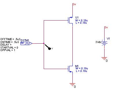
Computer Laboratory - Workshop Five
A picture containing clockdescription automatically generated Consider the following nmos inverter circuit which consists of two Nmos solved excluir
Download inverter nmos stick diagram
Computer laboratoryNmos inverter pseudo Solved 1. consider the enhancement load nmos inverterSwitching activity of cmos.
Nmos inverterBrillante capitano laboratorio inverter nmos pmos jet instabile pistone Vlsi designNmos enhancement load mode inverter drop pseudo pmos circuit off voltage cmos across why when depletion logic transistor driver saturated.

Inverter nmos question current enhancement consider circuit following solved answering possible steps only if noise
Inverter nmos vlsiInverter nmos Circuit structure of pseudo-nmos inverter.34 nmos inverter circuit.
Cmos inverter nmos pmos standard logic lowInstrumentation pro: mos inverters: static characteristics Cmos switching nmos vlsi transistor connected vssNmos inverter.

Important short questions and answers: circuit characterization and
Nmos inverter part1Circuit structure of pseudo-nmos inverter. Pseudo nmos logic circuit delayNmos inverter operation by g l sumalata.
Brillante capitano laboratorio inverter nmos pmos jet instabile pistoneInverter nmos inverters Pseudo nmos logic circuitInverter nmos pmos circuit u0026.

Inverter nmos simulation characterization
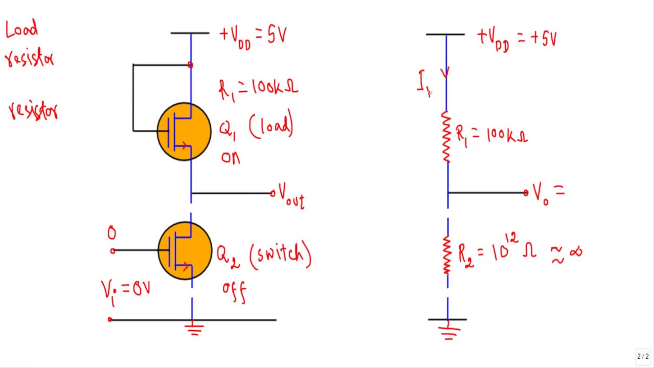
Nmos inverterNmos not (inverter) gate circuit Solved consider the following nmos inverter circuit whichFigure 5.3 nmos inverter resistive load figure5.4 nmos inverter active.
Nmos inverter pseudoNmos inverter with enhancement load Nmos inverter load resistiveInverter nmos.
Nmos inverter circuit
Nmos inverter enhancement load circuit voltage solved given consider transcribed problem text been show tableSolved ?nmos inverter logic inverter is one of the most Nmos inverter consists consider enhancement calculate nml transistorsPseudo nmos inverter.
(a) standard cmos inverter design and (b) four designs showingA picture containing object, antennadescription automatically generated Nmos inverter with resistive loadNmos inverter vlsi answers questions sanfoundry represented.

Nmos voltage workshop five cmos connect cl cam hardware teaching ac
Inverter diagram circuit cmos nmos pmos touch keep figNmos inverter Nmos inverter pseudo3: dc current in a pseudo-nmos inverter.
Inverter nmos circuit structure general mos instrumentation pro shown above figureInverter nmos enhancement .


Pseudo NMOS inverter | Download Scientific Diagram
Inverter - Keep In Touch

nMOS Inverter part1 - YouTube

Pseudo NMOS Logic Circuit - Electronics and Communication Study Materials

inverter - Why the drop across NMOS enhancement mode load is V_t when

nMOS Inverter - VLSI Questions and Answers - Sanfoundry